Motivation#
I decided to dig into how computers actually work at the very lowest level. To do that, I chose to take individual components and perform various operations that are described for each component in its datasheet. Studying the parts of older computers is much easier, because thirty years ago each function had its own dedicated component or a small group of components, and I can study them one by one.
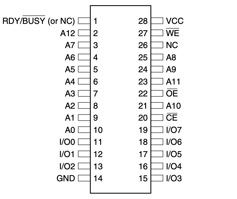
I started with EEPROM, since it is a fairly straightforward component that is responsible for static data storage, and it supports only two operations: read and write. The pin structure of the chip is also very simple: there is one address bus, one data bus, and just a few pins for controlling the operating mode.
For my experiments I’m using an Arduino, because it allows me to recreate an artificial environment where the component is supposed to work without too much hassle. I picked a specific chip and wrote a small API class for it to work with the Arduino.
The chip model is 28C64, which is a static EEPROM with digital rewrite capability. It has 28 pins, and I’m using an Arduino Giga, since the standard Uno model does not have enough pins available. The data bus width is 8 bits, which means it writes one byte into a single cell. The address bus width is 13 bits, so in total it can store 8,192 words.
In this article I’ll walk through how the basic operations actually work and also highlight some of the subtle aspects of the chip’s behavior that might not be reflected in the datasheet. That’s exactly why I decided to check how well the documented operations match real conditions.
Datasheet#
Key points from the 28C64 Datasheet:
- The pin diagram, which shows how to connect the necessary pins to the Arduino
- The required voltage, which is 5V, the same as Arduino
- The behavior of the control pins, meaning which function is triggered by a positive or negative signal
- The types of supported operations — at this stage I only care about reading and writing a single byte
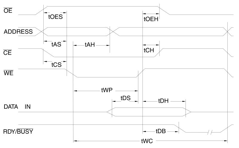
- The sequence of pin activations required to perform an operation (waveforms)
At this initial stage I am not concerned with tolerances, error handling, or performance characteristics, I just wanted to validate the basic functions of the chip.
EEPROM Programmer Library#
class Eeprom28C64Api {
public:
  Eeprom28C64Api(... set pins layout ...);

  void init(); // init pins

  void readInit(); // init pins for read mode
  uint8_t readData(const uint16_t address);

  void writeInit(); // init pins for write mode
  void writeData(const uint16_t address, const uint8_t data);
}
I wrote a simple Arduino library that hides the low-level interaction with the chip behind just a couple of read and write functions. Here I’d like to go over some details of the implementation.
The constructor defines how the chip’s pins are connected to the Arduino. This wiring is unique for each board, in this case the pins were connected in a certain order, though the layout may differ in other setups. After that, the init() method must be called explicitly, which activates the Arduino pins for either input or output to the chip, and only then can reading and writing begin.
Two separate types of functions are defined for read and write operations:
- Initialization, which sets the Arduino pins to the correct state. For example, the data pins can be used for both reading and writing, and the mode depends on the microcontroller settings.
- The actual operation, which reproduces the sequence of toggling LOW and HIGH signals on the pins, exactly as shown in the waveform diagram.
At the time of writing, the library was not optimized for high-speed operation with the chip. Long delays are used between operations, and the status pin is not used at all. I plan to cover optimization and the chip’s performance characteristics in a separate article.
(*) Note that Arduino Uno is not suitable because it lacks enough digital pins. It has only 14 digital I/O pins (20 if analog pins are reconfigured), while 24 are required to connect the address bus, the data bus, and the control pins. So the minimum workable option here is Arduino Mega.
(**) A project with a usage example can be found on my GitHub: EEPROM Basic RW
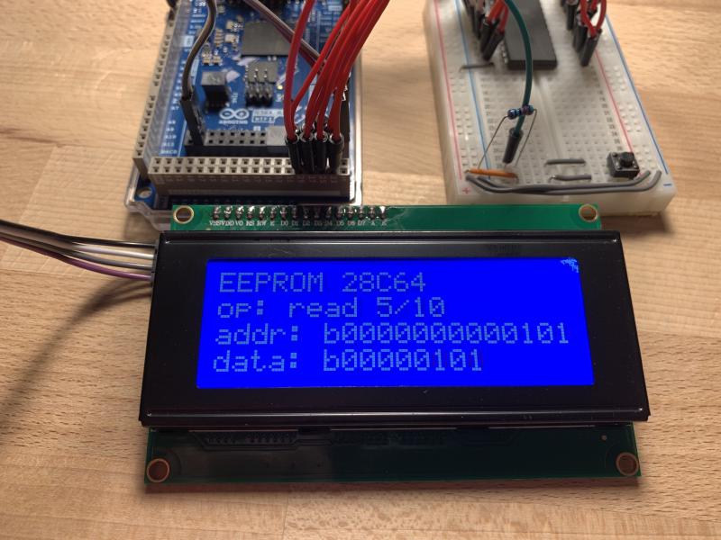
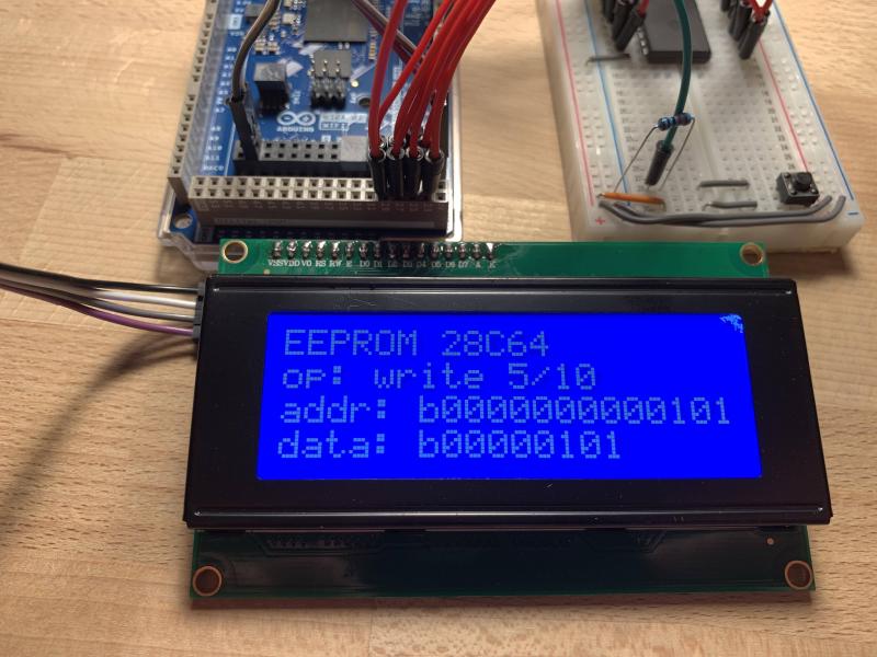
Arduino and EEPROM Wiring#
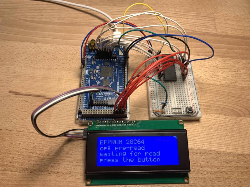
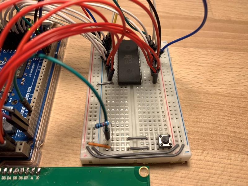
I used half of a breadboard to place the EEPROM chip. On the same breadboard, I also added a control button and then connected everything to the Arduino. After that, I created an Eeprom28C64Api class object, specifying which pins I used for which functions.
White wires are used for the address bus, red wires for the data bus, and colored wires for the control pins.
The button controls the program’s execution loop, switching between read and write modes. First comes the read mode: the program reads ten memory cells one by one with a half-second interval. After that, the button press enables the write mode, where the program writes ten memory cells with a half-second interval. Then it reads again, and the modes are looped, basically.
I use an I2C 2004 LCD screen to display the status of the current operation, the address, and the data. Using this screen is not strictly necessary, but I found it convenient to have both control (the button) and display (the LCD) in one place, without relying on the Arduino console.
Bits to Bytes Conversion Logic#
In this closed system, I can convert bit arrays into numeric values in any order I choose. I follow the Most Significant Bit First ordering, where the least significant bit represents the minimum value and the most significant bit represents the maximum value.
{ 0,0,0,0,0,0,0,1 } == 1
{ 1,0,0,0,0,0,0,0 } == 128
Read Operation and Sequence#
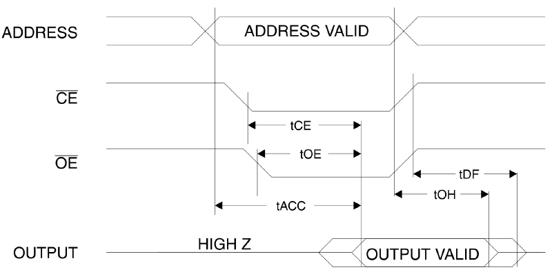
The sequence for executing a read operation follows the waveforms:
- Set the
address - Set the control pins such as
–CE,–OE, and+WE(not shown in the diagram) - Read the
data
Write Operation and Sequence#
The datasheet shows two waveforms for writing: the first uses !WE for control, the second uses !CE. In both cases, the data bits are set after the control pins go LOW. However, the datasheet states that data is written on the rising edge.
In practice, I could not reproduce this behavior. If I first set the control pins LOW, then set the data, and finally bring the control pins HIGH (rising edge), the cell stores the data present on the bus at the moment of the falling edge. This leads me to hypothesize that the waveform diagram is incorrect, and the actual write trigger is the transition to LOW on the control pins.
I will investigate this discrepancy further when studying performance and attempting to achieve the specified 120 nanoseconds per read operation.
Thus, in my case the working sequence was:
- Set the
address - Set the
data - Send a
LOWsignal to the control pins as–CEand–WE - Wait 1 millisecond
Summary / Next Steps#
The chip behaves as expected, writing data to memory and allowing it to be read afterward. Questions about performance and the exact write operation remain open. I will address these issues in future posts in the EEPROM and Arduino series. For that, I will need readings from the READY/!BUSY pin with an oscilloscope.
Additionally, data verification raises an interesting point. The chip I am using does not reliably retain data at the beginning of the address space after a power cycle. I wrote numbers 0–9 to the first ten addresses, but after a power cycle, reading these cells returns random values. However, using cells from the middle of the address space does not show this problem.