TLDR#
In this post, I summarize my observations of incorrect Arduino behavior made during debugging of the EEPROM Programmer project. The related post, EEPROM Programmer: Debugging Read Operations, describes the debugging process and the sequence of steps that led to identifying the root cause.
I connect external chips such as CPUs or EEPROMs directly to the Arduino and exchange digital signals with them. The resulting signal often resembles PWM, where the oscilloscope waveform appears as a series of narrow pulses. Complex chips expect this kind of pulsed signaling and can respond unpredictably to any other form of data exchange.
Improperly initialized Arduino pins distort the transmitted signal and can cause data corruption if the connected chip supports memory read and write operations. In this post, I present several examples of distorted data transmission and demonstrate how to quickly identify the problem using an oscilloscope. At the end, I explain how to properly connect the NC (Not Connected) pins of the chip to prevent parasitic noise from the Arduino from affecting the chip’s correct operation.
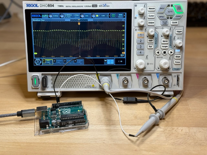
For the experiments, I used an oscilloscope with a single probe connected and an Arduino Uno R3 board. The post includes code examples, explanations of correct and incorrect behavior, and oscilloscope waveform screenshots for clarity.
Separately from the experiments, I analyze what happens during an Arduino reset, which signals appear on the pins and how they can affect externally connected chips.
“Initialized” and “Uninitialized” Pins Experiments#
I use a simple PWM signal loop to simulate digital data transmission. The experiment includes three tests with different signal switching speeds.
In the first case, the pin mode is correctly configured in Arduino’s setup() function, and the oscilloscope shows the expected result: clean voltage pulses switching between 0 V and 5 V, with only the frequency changing. In the second case, no mode is set for the pin, leaving it in an undefined state. In this configuration, the pin behaves unpredictably, with the output pattern varying depending on the frequency.
Additionally, I test how the pin behaves in a static HIGH or LOW signal. When the pin is properly initialized, it outputs a stable voltage level of 0 V or 5 V. However, if the pin is uninitialized, its behavior again becomes unpredictable.
PWM Signal Loop#
void setup() {
    // comment this line for the "uninitialized" experiment
    pinMode(13, OUTPUT);
}

void loop() {
    // low frequency, 10 ms
    // const int delay_us = 10000;

    // medium frequency, 1 ms
    // const int delay_us = 1000;

    // high frequency, 0.1 ms
    const int delay_us = 100;

    // PWM waveform
    delayMicroseconds(delay_us / 2);
    digitalWrite(13, 1);
    delayMicroseconds(delay_us / 2);
    digitalWrite(13, 0);
}
Initialized Pins#
When a pin is properly initialized, the PWM output produces uniform, clean pulses at any frequency. The durations of the 0 V and 5 V levels are consistent, forming flat, stable plateaus. This is how a correct digital signal should look. Below are oscilloscope waveform screenshots taken at different PWM frequencies and time/div scales for clarity.
Initialized Low Frequency PWM, 10 ms/div 👇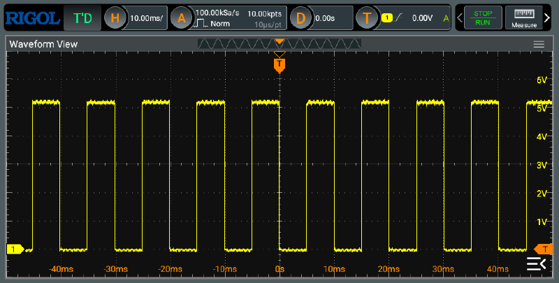
Initialized Medium Frequency PWM, 10 ms/div 👇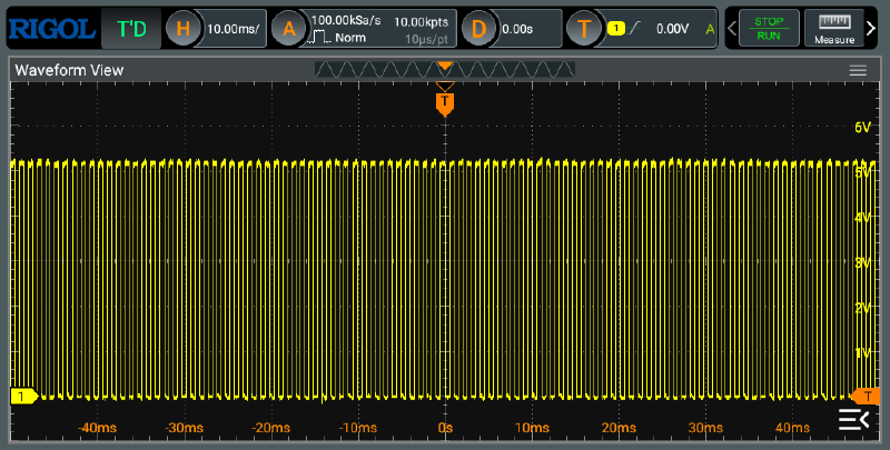
Initialized Medium Frequency PWM, 1 ms/div 👇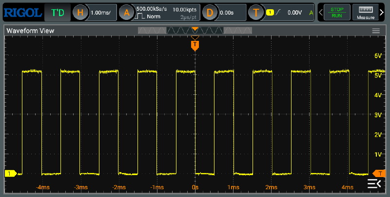
Initialized High Frequency PWM, 1 ms/div 👇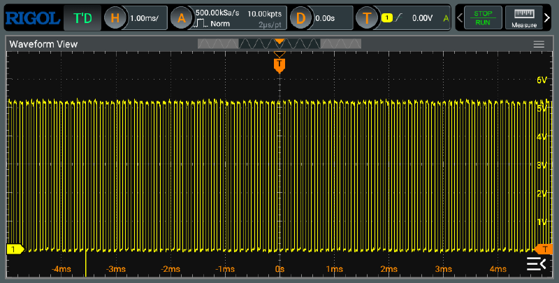
Initialized High Frequency PWM, 0.1 ms/div 👇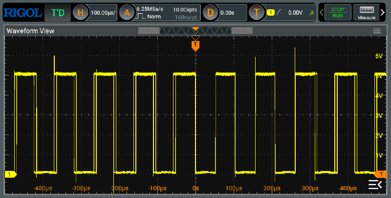
Uninitialized Pins#
Uninitialized pins behave differently at various frequencies. The higher the frequency, the harder it is to recognize the original signal shape, and the lower the chance that an external chip—such as a CPU or DAC—can tolerate the distortion. A general pattern can be observed: the signal drifts, which becomes visible at larger time/div values. The upper part remains relatively stable around 5 V, while the lower part turns into a sine-like waveform and never reaches 0 V. As the modulation speed increases, the waveform becomes more compressed.
Uninitialized Low Frequency PWM, 100 ms/div 👇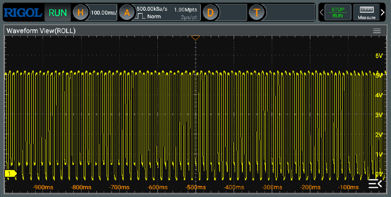
Uninitialized Low Frequency PWM, 10 ms/div 👇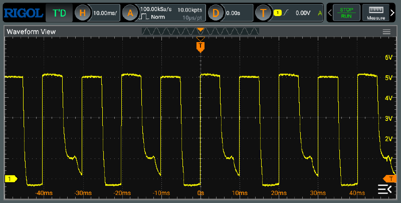
At low frequencies, the digital nature of the signal is still somewhat recognizable, but the pattern is unstable. The lower edge is jagged, with full pulses alternating with shorter ones in a sinusoidal rhythm, clearly visible at 100 ms/div.
Uninitialized Medium Frequency PWM, 10 ms/div 👇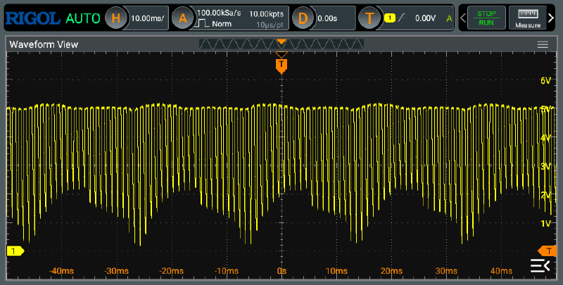
Uninitialized Medium Frequency PWM, 1 ms/div 👇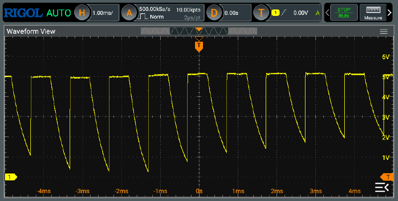
At medium frequencies, this effect becomes more pronounced. The plateau near 0 V disappears, giving the waveform a sawtooth shape. The drifting lower-edge pattern becomes clearer at 10 ms/div.
Uninitialized High Frequency PWM, 1 ms/div 👇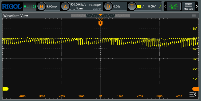
Uninitialized High Frequency PWM, 0.1 ms/div 👇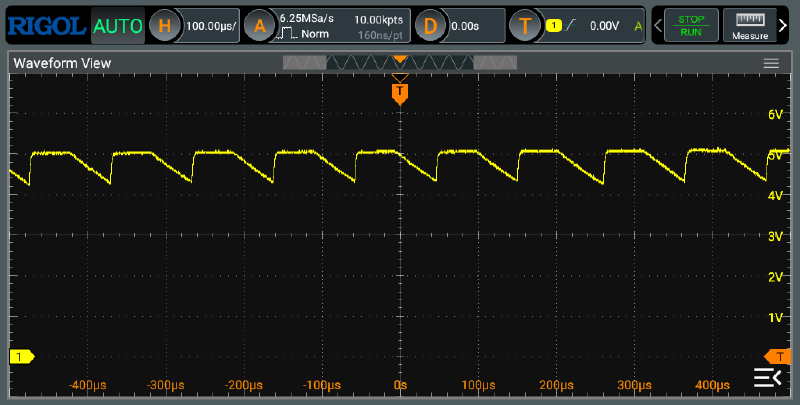
At high frequencies, the waveform turns into a sawtooth pattern near the 5 V level. The characteristic digital pulse pattern completely disappears. In this case, an external chip would interpret the signal as a constant HIGH at best, or as noise affecting the entire circuit at worst.
Note, that this is not a bandwidth limitation of the oscilloscope — waveform from a properly initialized pin at the same speed and scale shows a clean pulsed pattern, see the waveform example in the “Initialized Pins” section above.
Stable HIGH or LOW Signal#
void setup() {
    // comment this line for the "uninitialized" experiment
    pinMode(13, OUTPUT);

    digitalWrite(13, HIGH);  // or LOW
}

void loop() {}
Initialized Pins#
Properly initialized pins with stable values behave exactly as expected, outputting 5 V or 0 V depending on the digital signal applied to the pin—no surprises or deviations. When examined closely at low time/div values, small fluctuations within about 100 mV can be seen. These are likely background noise from the frequency generator. External digital devices are generally insensitive to this level of signal variation and do not interpret it as logic changes between 0 and 1.
Initialized HIGH signal, 50 ms/div 👇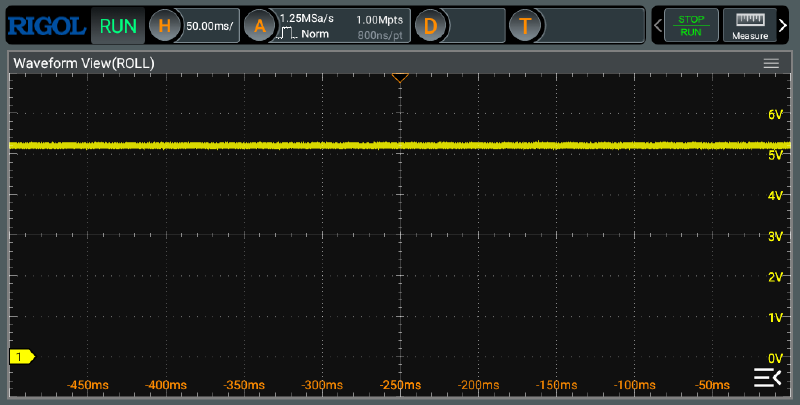
Initialized HIGH signal, 10 ms/div 👇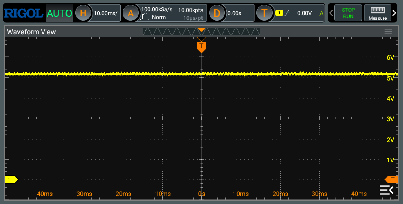
For an initialized pin, noise fluctuations are the same for both HIGH and LOW levels and remain within 50–100 mV, which is negligible at a 5 V signal scale.
Initialized LOW signal, 50 ms/div 👇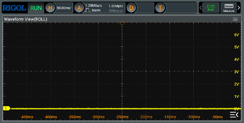
Initialized LOW signal, 10 ms/div 👇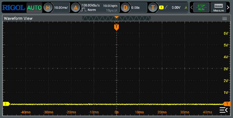
Uninitialized Pins#
The behavior of uninitialized pins differs significantly between HIGH and LOW states.
Uninitialized HIGH signal, 50 ms/div 👇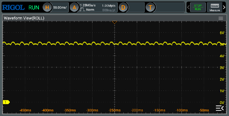
Uninitialized HIGH signal, 10 ms/div 👇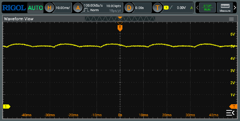
When driven HIGH, the signal pattern becomes irregular and the amplitude of fluctuations increases, but it still remains within the 5 V range, with variations up to about 200 mV. External chips would still interpret this as a valid HIGH signal.
Uninitialized LOW signal, 50 ms/div 👇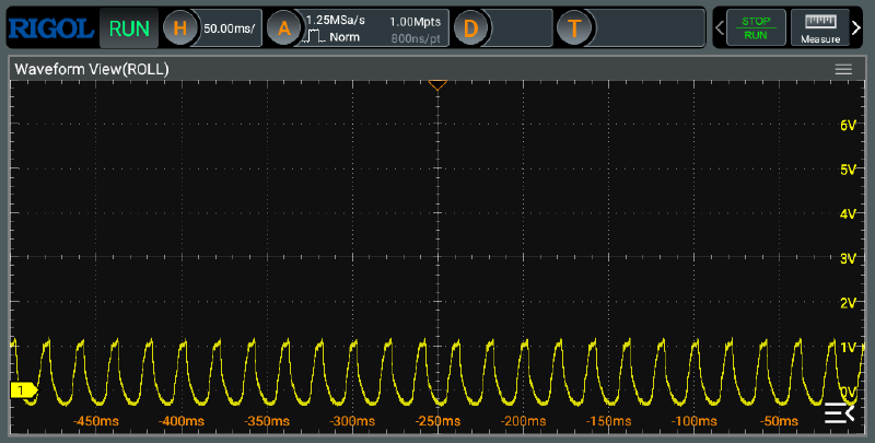
Uninitialized LOW signal, 10 ms/div 👇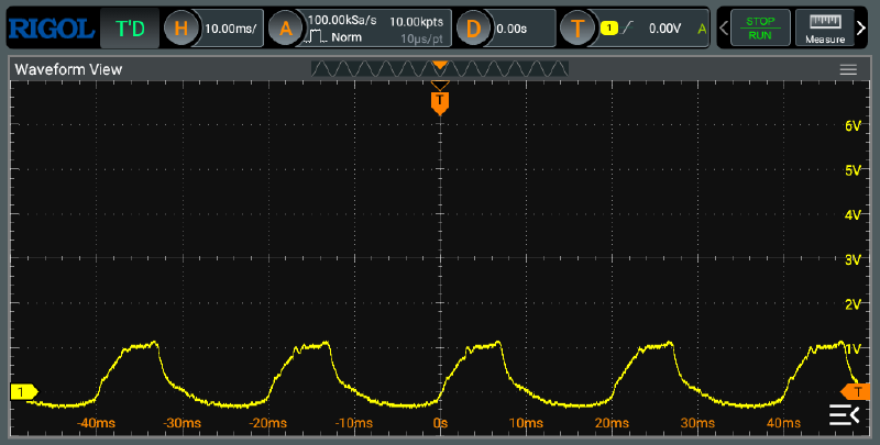
In the LOW state, the amplitude of fluctuations increases to about 1 V, while the same background noise pattern observed on initialized pins remains. Oscillations between 0 V and 1 V can be interpreted by an external chip as transitions between HIGH and LOW, potentially causing unpredictable behavior.
While the board outputs a stable LOW signal, an external device—such as a DAC—may interpret this noise as a sequence of 0–1 transitions and produce unintended output patterns or audible artifacts.
I analyze the behavior of an uninitialized pin in more detail in one of the following sections, explaining why a board reset can cause data corruption in a connected EEPROM chip.
How to Initialize NC Chip Pins#
Many integrated circuits include Non-Connected (NC) pins as part of their specification. For example, the AT28Cxx family of EEPROM chips shares the same package form factor across models with different memory sizes. In lower-capacity versions, the higher address bits are unused and are therefore marked as NC.
The same chip family defines different connection modes for different operating states. For example, the !BSY pin should remain NC during read operations, but during write operations it outputs a signal indicating the completion of the write cycle. In this case, the connection type for this pin must be controlled programmatically.
As discussed above, leaving such pins uninitialized can cause unpredictable and sometimes destructive behavior. The question is how to properly initialize an NC pin. Community guidance often suggests INPUT_PULLUP, I compare it with OUTPUT mode driven LOW and evaluate the chip’s behavior.
The following example is taken from the codebase of my EEPROM Programmer project.
// INPUT_PULLUP
pinMode(_nonConnectedPins[i], INPUT_PULLUP);

// OUTPUT + LOW
pinMode(_nonConnectedPins[i], OUTPUT);
digitalWrite(_nonConnectedPins[i], LOW);
Uninitialized NC Pin, 500 us/div 👇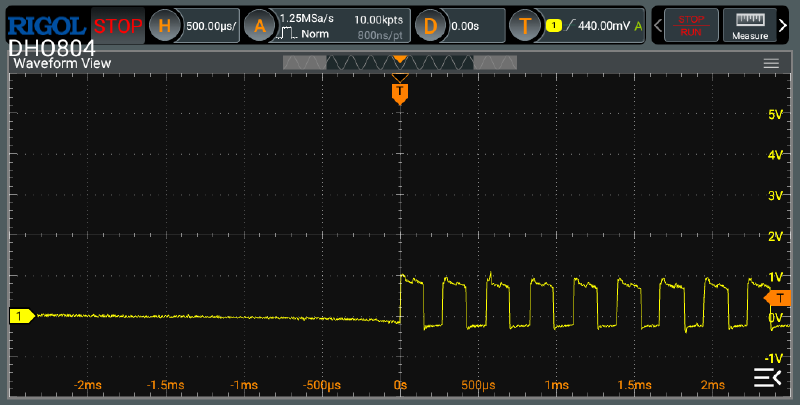
Potentially destructive behavior: an uninitialized pin picks up crosstalk from adjacent pins during read and write operations. The induced excursions are on the order of 1 V and match the toggling pattern of the neighboring address pin. It is unclear whether this unexpected signal on the NC pin affects device operation, but the behavior does not look safe.
INPUT_PULLUP NC Pin, 500 us/div 👇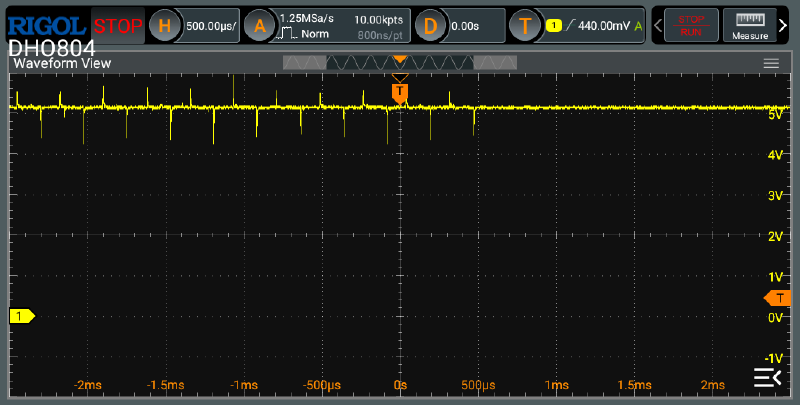
Using INPUT_PULLUP mode works, but it drives the NC pin HIGH, while many datasheets recommend tying NC pins to GND. I have not observed adverse behavior with INPUT_PULLUP; in fact, I migrated all EEPROM Programmer interfaces to this scheme. It functions correctly, though the mismatch with the GND recommendation is counterintuitive.
Additionally, the waveforms show noise in the form of positive and negative spikes up to 1 V. This noise appears consistent with crosstalk from adjacent pins during device operation and, in pattern, resembles the noise observed on an uninitialized pin.
OUTPUT mode and LOW signal NC Pin, 500 us/div 👇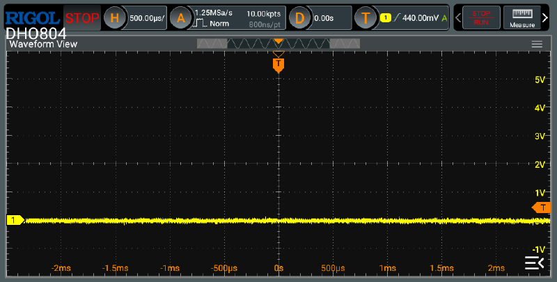
Using the OUTPUT mode with a LOW signal produces the most predictable and consistent results. No crosstalk noise from adjacent pins is observed, and the NC pin is held at 0 V, effectively tied to GND, which aligns with the device specifications.
How Arduino Behaves During the Reset#
I apply a PWM pulse with a 12 ms period to three pins, each with a slight phase offset, to make the reset cycle visible against the normal 5 V operating amplitude. The reset cycle, triggered by the onboard button, lasts about 1.7 seconds on the Arduino Uno R3. During this period, all pins behave identically, entering the uninitialized state described in the previous section and showing a sawtooth waveform with an amplitude of approximately 1 V.
Full Reset Cycle for 3 Pins, 200 ms/div 👇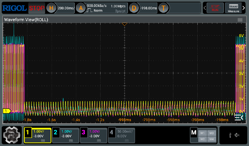
The graph shows no significant phase shift between the sawtooth waveforms of different pins during the reset cycle. Transitions between 0 V and 1 V occur at nearly the same time across all pins throughout the entire reset period.
End of the Reset Cycle for 3 Pins, 5 ms/div 👇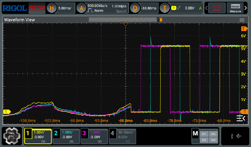
At the end of the reset cycle, pin initialization restores them to the normal operating state, and they resume generating the correct 0–1 pulse sequence with a slight phase offset, as programmed. The small spikes on the blue trace are most likely due to oscilloscope probe miscalibration.
Yellow is the management LED_BUILTIN pin, 200 ms/div 👇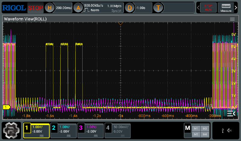
The behavior of the LED_BUILTIN pin 13, which drives the onboard LED, differs from that of other pins on the Arduino Uno. For most of the reset cycle time, the LED pin remains initialized, with two short periods of indeterminacy at the beginning and end of the cycle.
Additionally, the board uses pin 13 to signal the reset process by sending three consecutive pulses at the start of the cycle. This is likely one reason why pin 13 should not be used for interfacing with external devices, as the board reserves it for its internal operations.
End of the Reset Cycle for the management LED_BUILTIN pin, 20 ms/div 👇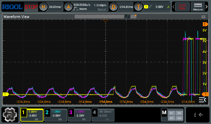
This graph shows that the duration of a single sawtooth cycle is approximately 20 ms, resulting in about 85 oscillations between 0 V and 1 V over the 1.7-second full reset cycle.
This is the most critical observation: an external connected chip may interpret voltage transitions between 0 V and 1 V as legitimate digital signal changes and execute corresponding operations according to its datasheet.
As a result, during a full reset cycle, the external chip can receive up to 85 false operation signals. Because the waveforms on different pins are only slightly phase-shifted, these signals can resemble valid command sequences supported by the device.
In practice, this leads to data corruption on the connected EEPROM 28C64, which can overwrite about 20 random memory cells during a single reset cycle. I will discuss this issue in more detail in one of the upcoming posts.